
Н. Э. Баумана Стасенко И. В., Кальгин Ю. А обучение чтению литературы на английском языке по специальности рл6 «Основы нанотехнологии» Учебно-методическое пособие
| Вид материала | Учебно-методическое пособие |
- Учебно-методическое пособие по курсу a handbook with resource material for the course, 711.05kb.
- Муниципальное общеобразовательное учреждение средняя общеобразовательная школа №18, 236.35kb.
- Учебно-методическое пособие Нижний Новгород 2010 федеральное агенаство по образованию, 1470.01kb.
- Учебно-методическое пособие Нижний Новгород 2010 министерство образования и науки, 1469.96kb.
- Одобрено учебно-методическим советом факультета фмэит страноведение на английском языке, 393.67kb.
- Обучение чтению на английском языке в старших классах якутской школы (базовый уровень), 368.57kb.
- Учебно-методическое пособие для студентов всех форм, 757.37kb.
- Учебно-методическое пособие для студентов дневного и заочного отделений специальности, 381.12kb.
- Сагимбаев Алексей Викторович учебно-методическое пособие, 1354.91kb.
- Учебно-методическое пособие для студентов естественных специальностей Павлодар, 1215.72kb.
Text 2A
Introduction. Nanomaterials with 2D-nanostructures (nanolayers)
2D-nanostructures are structures like layers, having large (near 1 μm) sizes on two coordinate axes, and nanometer size on third axe.
Lateral AlGaAs- superlattice
Abundant new physics was brought about by the invention of the superlattice (SL) concept and its subsequent realization through molecular beam epitaxy (MBE) of layered semiconductor structures with atomic precision. The formation of minibands isolated by minigaps in the vertical SL direction ensues from the coupling between adjacent quantum wells. In order to reduce the dimensionality of the system, electrons are confined in one direction to a quantum well, and a lateral periodic potential modulation may additionally be imposed from the surface of the sample with, for example, lithographically defined top gates. As in the conventional vertical SL geometry, an artificial band structure derives from the reduced width of the Brillouin zone and zone folding. Magnetotransport offers an excellent tool for the study of the resulting band structure in these laterally modulated two-dimensional systems (2DES), since oscillations in the magnetoresistance provide immediate information on the area encircled by closed electron orbits at the Fermi energy EF. Such experimental evidence for an artificial band structure is sparse. Only very recently, using two-dimensional modulation, unambiguous proof of two different closed electron orbits was achieved. This lack of evidence may be related to the inherent inadequacy of lateral modulation schemes in producing concurrently a high quality 2DES and a sufficiently short period and large amplitude modulation to guarantee the occupation of only few, well-isolated minibands.
We use a new concept to fabricate lateral SLs based on the cleaved edge overgrowth technique, that overcomes the limitations of previous geometries by periodically modulating the material composition directly adjacent to the 2DES. In this way, both the period and the modulation strength can be tailored with unprecedented precision by MBE growth. In a first MBE step, an undoped SL with lattice constant d=100 nm of 30 periods of 50 nm GaAs and 50 nm Al0.32Ga0.68As is grown between two n-GaAs contacts, that act as source and drain. In a second MBE step, the sample is cleaved in situ and immediately thereafter overgrown by a 30 nm undoped GaAs layer, a 100 nm AlAs barrier, and an n-GaAs gate contact. By applying a positive gate voltage with respect to source and drain a 2DES is induced at the GaAs/AlAs heterointerface. The finite overlap of the electron wave function with the SL causes a modulation of the electron density ns in x direction with a strength that depends on the GaAs layer thickness. For our sample this variation of the density, integrated over the z direction, exceeds 10%, as determined by a self-consistent 2D-Poisson/Schrödinger calculation. (2474)
Answer the following questions:
1) What is a 2-D nanostructure? 2) How was the new physics brought about? 3) In what way was the dimensionality of the system reduced? 4) Why does magnetotransport offer an excellent tool for the study of the resulting band structure in laterally modulated 2DES? 5) What was the difficulty in understanding of the resulting band structure in laterally modulated two-dimensional systems? 6) Why is a new concept to fabricate lateral SLs based on the cleaved edge overgrowth technique?
Task 1. Look through the text again carefully and explain the difficulty in understanding of the resulting band structure in laterally modulated two-dimensional systems?
Task 2. Describe the process of the lateral SL fabrication in detail and draw the picture of the process in a stepwise manner.
Task 3. Use your background knowledge of physics and the information given in the text to explain the terms Brillouin zone and Fermi energy.
Task 4. Use Internet to find more information about the new concept on super lattice fabrication and present it.
Task 5. Give the summary of the text mentioning the process of the lateral SF fabrication.
Memorize the following basic vocabulary and terminology to text 2B
- heterojunction – неоднородный переход в полупроводниковом приборе, гетероструктурный переход;
- intrinsically limited by optical photon scattering – по своей природе ограничен оптическим рассеянием фотонов;
- electron density – плотность электронов;
- enhance channel conductivity – повысить проводимость в канале;
- conduction band – смещение зоны проводимости;
- metallographic vapor phase epitaxy – металлографическая эпитаксия из паровой фазы
- electron sheet density – пленочная плотность электронов;
- subband occupancy – заселенность в подзоне;
- electro charge distribution – распределение заряда электронов;
- quantum wells (QW) – квантовые ямы;
- intersubband scattering – внутреннее рассевание в подзоне;
- light-induced destruction – разрушение вызванное светом
- charge correlation – зарядовая корреляция (взаимосвязь);
Read text 2B and answer the questions after the text
Text 2B
InAlGaAs layers for high electron mobility transistors
Mobility of carries in quasi two-dimensional electron gas (2DEG) formed at a semiconductor heterojunction is intrinsically limited by optical phonon scattering at room temperature. For high performance devices, an increase in electron density leads to enhanced channel conductivity. The existence of DX centers in AlxGa1–xAs (x>0.22) restricts the use of a high Al mole fraction in AlxGa1–xAs /GaAs heterostructures. The small conduction band offset in such structures limits the electron density below 1012 cm–2. Owing to larger conduction band offset the pseudomorphic GaAs/InxGa1–xAs/AlyGa1–yAs quantum wells (QWs) have attracted much interest in high-speed devices. The best samples of those structures with very high 2DEG mobilities are usually grown by molecular beam epitaxy (MBE). Recent progress in metalorganic vapor phase epitaxy (MOVPE) has led to growth of high quality heterostructures. Additionally, δ-doping increases the electron density and mobility of 2DEG in the QW, and consequently improves device performance.
GaAs/In0.2Ga0.8As/Al0.2Ga0.8As QW grown by MOVPE at 630 °C and consisted nominally of 600 nm GaAs buffer layer, followed by 90 nm of (5 nm Al0.2Ga0.8As/5 nm GaAs) superlattice, 310 nm of 205 nm GaAs top barrier. The Si δ-doping (nD=2.3*1012 cm–2) was placed 10 nm from the QW in the back Al0.2Ga0.8As barrier. Similar δ-doping was applied 2 nm below the structure surface in order to saturate the surface states.
The high electron mobility 2DEG was formed in the investigated structure with no significant parallel conduction. Nonmonotonic dependence of both transport and quantum mobilities on electron sheet density was observed with the maximum related to the onset of the upper subband occupancy. An apparent increase of the quantum mobility was explained by the ionization of deep centers in the top barrier which changed the QW from asymmetric to the more squarelike. The resulting shift of the electron charge distribution away from the δ-layer leads to an increase of electron transport mobility in the QW. An explanation of the quantum mobility decrease after the upper subband occupation is less straightforward. The intersubband scattering presumably present in this density region has the opposite effect on the quantum mobility than the more effective remote charge screening. Moreover a light-induced destruction of charge correlations may be important. (2090)
Answer the following questions:
1) Why is the mobility of carriers in quasi two-dimensional electron gas intrinsically limited? 2) Why did pseudomorphic quantum well attract much interest in high-speed devices? 3) What is the technique to obtain the structures with very high 2DEG mobilities? 4) How was an apparent increase of the quantum mobility explained? 5) What leads to the increase of electron transport mobility in the quantum well?
Task 1. Use your background knowledge and explain the need for high electron mobility transistors. How was it achieved?
Task 2. Explain the structure of GaAs/In0.2Ga0.8As/Al0.2Ga0.8As quantum well and draw a stepwise scheme of its growth by metalogranic vapor phase epitaxy.
Task 3. Look through the second part of the text carefully and explain the characteristics of the high quality heterostructure.
Memorize the following basic vocabulary and terminology to text 2C
- inherent property – внутреннее свойство;
- increase luminescence efficiency considerably – значительно увеличить выход люминесценции;
- saturation velocity – скорость насыщения;
- wurtzite6 – вюртцит;
- Monte Carlo method7 – метод Монте Карло (совокупность математических методов, позволяющих найти желаемое решение путем статистических испытаний, выполняемых, как правило, при помощи ЭВМ)
- drift velocity – скорость смещения, дрейфа;
- superior characteristics – более высокие характеристики;
- overshoot velocity – скорость проскакивания;
- field effect transistor – транзистор, управляемый полем;
- cutoff frequency – предельная частота;
- high-speed high-performance heterojunction – высокоскоростной высокоэффективный гетеропереход;
- pulsed laser deposition technique – метод осаждения импульсным лазером;
- impurity – примесь;
- Hall mobility – холловская подвижность, подвижность зарядов;
- molar ratio – молярная концентрация; мольное отношение;
- enhanced decomposition – повышенное (усиленный) разложение, распад;
Read text 2C and answer the questions after the text
Text 2C
InN layers for high electron mobility transistors
Developments in the field of III-nitride (InN, GaN, and AlN) semiconductors have been spectacular due to their highly attractive inherent properties. During the last few years the interest in the InN has been remarkable. Recent results indicate that the InN films almost meet the requirements for application to practical devices. The development in blue/ultraviolet (UV) light emitting diodes (LEDs) and laser diodes (LDs), and also high-frequency transistors operating at high powers and temperatures has proved the benefits of the nitride materials system. Indium nitride (InN) is an important III-nitride semiconductor with many potential applications. The use of InN and its alloys with GaN and AlN makes it possible to extend the emission of nitride-based LEDs from ultraviolet to near infrared region. For example, along with GaN, the InN ternary alloy, InGaN, has found application in a variety of heterostructure based optoelectronic devices, such as LEDs and lasers. The InGaN quantum wells are indispensable for light emitting devices because incorporation of small concentrations of In in the active GaN layer increases luminescence efficiency considerably.
InN was predicted to have lowest effective mass for electrons in all the III–nitride semiconductors, which leads to high mobility and high saturation velocity. The theoretical maximum mobility calculated in InN and GaN at 300 K are about 4400 and 1000 cm2/(V*s), respectively, while at 77 K the limits are beyond 30 000 and 6000 cm2/(V*s), respectively. The electron transport in wurtzite InN was studied using an ensemble Monte Carlo method. It was found that InN exhibits an extremely high peak drift velocity at room temperature. The saturation velocity is much larger than that of gallium arsenide (GaAs) and gallium nitride (GaN).
InN achieves the highest steady-state peak drift velocity: 4.2*107 cm/s. This contrasts with the case of GaN, 2.9*107 cm/s, AlN, 1.7*107 cm/s, and of GaAs, 1.6 *107 cm/s. It was concluded that the transport characteristics of InN are superior to those of GaN and GaAs, over a wide range of temperature from 150 to 500 K and a doping concentration up to 1019 cm–3. The transport characteristics were shown to be relatively insensitive to variations in temperature and doping concentration, unlike GaAs. This suggests that there may be distinct advantages offered by using InN in high frequency centimeter and millimeter wave devices.
The transient electron transport, which is expected to be the dominant transport mechanism in submicron-scale devices, was also studied in InN. It is found that an InN exhibit the highest peak overshoot velocity and that this velocity overshoot lasts over the longest distance when compared with GaN and AlN. It was predicted that InN-based field-effect transistors (FETs) have an extremely high speed with a cutoff frequency of over 1 THz for 0.1 mm gates. Thus, InN is a highly potential material for the fabrication of high-speed high-performance heterojunction FETs.
As-grown InN is always n-type with a very high background carrier concentration-an observation similar to GaN before better doping control of that material was achieved. However, there is only one report of p-type InN grown by the pulsed laser deposition (PLD) technique, which to date has never been reported in as-grown InN film or even intentionally doped InN film. There has been much speculation as to what species is responsible for high background donor concentration in the grown InN. Theoretical calculation as well as experimental result gives conflicting views and opinions regarding the major reason responsible for such high n-type conductivity. The potential candidates for such high background donors are native defects, such as N vacancy, nitrogen antisite, and impurities, such as ON, SiIn , and possibly interstitial H. According to the oldest and common view, the nitrogen vacancy is the most probable reason for n-type conductivity of InN.
Selection of GaN for the underlying layer and increased InN film thickness significantly improve the Hall mobility. A Hall mobility of about 700 cm2/(V*s) was obtained in the InN film grown on GaN even at an electron concentration of 5*1019 cm–3. A high NH3/trimetilindium (TMI) molar ratio and enhanced NH3 decomposition (by growth temperature, atmospheric pressure growth, reduced flow velocity, etc.) significantly improved the electrical properties of MOVPE grown InN film. As a result, a carrier concentration in the order of 1018 cm–3 was obtained and the highest electron mobility obtained was 730 cm2/(Vs). These are the best electrical properties ever achieved in the MOVPE grown InN film. (3989)
Answer the following questions:
1) Why have the developments of III-nitride semiconductors been spectacular? 2) What do recent development results indicate? 3) What proved the benefits of the nitride material system? 4) What is the application of the III-nitride semiconductor? 5) Why are the InGaN quantum wells indispensable for light emitting devices? 6) What was found by the ensemble Monte Carlo method? 7) What do the highest steady-state peak drift velocity and relatively insensitive transport characteristics suggest? 8) What was found while studying InN transient electron transport mechanism? 9) Why do the experimental results give conflicting views and opinions? 10) Due to what factors was the highest electron mobility obtained?
Grammar exercises
Exercise 1. Translate the following sentences paying attention to Participle Constructions in different syntactic functions.
- A metal disk implanted in the semiconductor distorts the electric field lines.
- Implanted in the semiconductor, a metal disk distorts the electric field lines.
- Spintronic memory being based on magnetic, semiconducting nanoparticles can be used in the future to produce nanostructured computer.
- Being based on magnetic, semiconducting nanoparticles, spintronic memory provides a promising direction to a nanostructured computer.
- A voltage applied across the ends of a semiconductor slab (пластина) sets up an electric field.
- If applied across the ends of a semiconductor slab, a voltage sets up an electric field, the latter causing randomly moving electrons to drift along the slab.
- The concept of photonic crystals having been theoretically formulated was used later to produce the first photonic crystal.
- The concept of photonic crystals having been theoretically formulated, the first photonic crystal was fabricated much later.
- Scientists created new nanomaterials, the latter having tunable electronic properties. The properties of these new nanomaterials being strongly dependent on their location along the nanotube, these new nanomaterials are believed to have far-reaching prospects to design single-molecule devices.
- The properties of nanomaterials being strongly dependent on their location along the nanotube make these materials suitable for single-molecule devices.
Exercise 2. Point out Adverbial Participle constructions and Absolute Participle constructions in the following sentences, translate them accordingly.
- If tested successfully, this particular vibration isolation will be adequate for the modern hardware developed recently.
- Being one of the best known solid–state devices, the Hall Effect sensor is still attracting considerable attention of scientists.
- The temperature increasing, no degradation of the sensor is observed.
- Structural approaches of nanotechnology facilities having been discussed, scientists came to the conclusion that nanotechnology requires extremely stable environment.
- Being based mainly on silicon or semiconductors, the conventional Hall Effect sensors have a remarkably low cost.
- Vibration environments having been explored, researches could provide manufactures with advanced nanotechnology.
- Environment permitting, nanomechanisms will work almost perfectly under these conditions.
- The needs of the users having been correctly assessed, nanotechnology designers focused their attention on good vibration environments.
- Though situated in a relatively quiet location, the equipment still needed a reliable internal vibration isolation.
- If developed, new technologies will be used for measuring nanoscale forces and dimensions.
- Appropriate nanotechnology criteria having been specified due to thorough research, scientists cannot always incorporate them in nanotechnology facilities.
- Being successfully used in memory circuits, resonant tunneling devices deserve special attention in the context of this report.
- The field lines and the current flow being concentrated through the metal disk, the more current flows through the device than when the disk is absent.
- Gold disks were embedded in one-millimeter-radius disks, the gold disks being about 1.5 microns thick.
- The size of a bit of information on a magnetic disk being reduced to increase storage density, the sensitivity of read-head must also increase.
- Being fabricated from nonmagnetic materials, the read heads would not suffer from magnetic noise limitations.
- Discovered in Japan, carbon nanotubes are divided into two basic types: single-walled nanotubes (SWNTs) and multiwalled nanotubes (MWNTs).
- Being hollow, nanotubes are lightweight, transparent to visible light and are excellent conductors of electricity.
- Though first demonstrated in nanotube transistors in the late 1990, nanotubes were first commercially used as structural reinforcements in composites and in lithium-ion batteries.
- The temperature rising from absolute zero to 78000 K, disintegration of a double-wall nanotube happens.
- Made of structures designed at the molecular level, DNA (deoxyribonucleic acid) machines with moving parts could be employed as nanomechanical sensors, switchers as well as for more elaborate robotic functions.
- Environmental vibration being reduced, the images produced by the scanning tunneling microscope (STM) become much better.
LESSON 3
Memorize the following basic vocabulary and terminology to text 3A
- Hall effect sensors – датчики Холла; датчики, работа которых основана на явлении Холла;
- proximity switches – бесконтактный переключатель;
- harsh environmental conditions – суровые природные условия;
- heterojunction – гетеропереход;
- band gap – запрещенная зона;
- intrinsic carriers – собственные носители заряда;
- elevated temperatures – повышенная температура;
- to sacrifice in mobility – снижение подвижности;
- breakdown voltage – напряжение пробоя;
- sheet carrier densities – пленочная плотность заряда;
- residual charge – остаточный заряд;
- annealed contacts – отожженные контакты;
- to dice – нарезать кристаллы из полупроводниковой пластины;
- biasing current – ток смещения, ток подмагничивания;
- linear regression fitting technique – метод линейно-регрессионного приближения;
Read text 3A and answer the questions after the text
Text 3A
AlGaN/GaN heterojunction for Hall Effect sensors
Hall effect sensors are widely used as proximity switches, position sensors, velocity sensors, and in current sensing applications. Although it is one of the best known solid-state devices, the Hall effect sensor is still attracting considerable attention. One of the areas of interest is to enable Hall effect sensors to function at high temperatures (>250 °C) and other harsh environmental conditions; those operating conditions are of prime importance for a wide range of industrial and military applications. Conventional Hall effect sensors are mainly based on silicon or compound semiconductors, such as InAs, InSb, and GaAs. The advantage of using silicon as the active layer of a Hall effect sensor is its easy integration with signal-conditioning circuits and its low cost. InAs, InSb, GaAs, and related heterojunctions typically have very high electron mobilities. As a result, Hall effect sensors based on these materials can have fairly high magnetic field sensitivity at low temperature up to room temperature. However, due to the narrow band gap of these materials, thermal activation of intrinsic carriers can significantly change their transport properties at higher temperature (>200 °C).
The resulting large temperature cross sensitivity makes these sensors unusable at temperatures above approximately 200 °C. By heavily doping the active layer, the extrinsic state of these semiconductors may be maintained to somewhat elevated temperatures; however, due to a sacrifice in carrier mobility, this approach is quite limited. Currently most Hall effect sensors on the market have a peak specified operation temperature of 200 °C or lower. AlGaN/GaN heterostructures have been a subject of intense investigation recently due to their high potential to be used for high temperature, high power radio frequency (rf) electronics.
The wide band gap of GaN-related materials leads to low intrinsic carrier concentration and high breakdown voltage, which is a requirement for extremely high microwave or millimeter wave power applications. Further contributing to the outstanding performance of AlGaN/GaN-based heterojunction transistors is their ability to form a two-dimensional electron gas (2DEG) with sheet carrier densities of 1013 cm−2 or higher near the interface without intentional doping. This is well in excess of those achievable in most other III-V material systems. It has been demonstrated previously that the spontaneous and piezoelectric polarizations play an important role on the 2DEG formation and confinement at the AlGaN/GaN interface.
The AlGaN/GaN heterojunction structures were grown by metal organic chemical vapor deposition on sapphire substrates. The epitaxial layer consisted of a 2 μm undoped GaN buffer layer and a 25 nm Al0.3Ga0.7N barrier layer. A sheet resistance of 250 Ohm/sq was obtained from Leighton measurement at room temperature. A capacitance voltage profile showed a 2DEG at the junction interface and no residual charge was found in the AlGaN barrier or the GaN/sapphire interface.
Square-shaped Hall devices were defined by optical photolithography followed by mesa etching using an inductively coupled plasma reactive ion etching system in a chlorine-based plasma. Ti/Al/Mo/Au Ohmic contacts were deposited by electron beam evaporation and annealed at 800 °C for 1 min. The processed wafer was diced into 3x3 mm2 chips. Each chip was mounted on top of a resistive heater element using high temperature epoxy. The combined assembly was mounted onto a chip carrier for testing. The heater element was used to raise and maintain the surface temperature of the Hall sensor and was calibrated using a high-precision infrared camera.
The output Hall voltage of the AlGaN/GaN Hall effect sensor as a function of temperature and magnetic induction curves have good linearity and are very close to one another from room temperature up to 300 °C. With increasing temperature, no degradation of functionality of the sensor is observed. In fact, the Hall voltage is larger at higher temperatures, which is shown by the larger slope at higher temperatures. As the measurements suggest, 300 °C is not a limiting temperature for operation. The magnetic induction and biasing current were fixed at 1.7 kG and 3 mA, respectively. The current-related magnetic sensitivity increases from approximately 54.5 to 56.5 V/(A*T) between room temperature (RT) and 300 °C. Using a linear regression fitting technique, the temperature coefficient of magnetic sensitivity is calculated to be 103 parts per million (ppm)/°C. This is an excellent value even for conventional Hall effect sensors made for low temperature operation. (3997)
Read text 3B and translate the text
Text 3B
CoFe/AlOx- nanolayers for magnetic tunnelling transistors
Recently, many researchers have investigated spin valve structures with nano-oxide layers (NOLs) or specular spin valves (SSVs) in the current-in-plane (CIP) configuration. But they have found many serious problems in achieving a sufficient quality for read head device applications with a density of over 300 Gbit in−2. In these structures, the giant magneto-resistance (GMR) sensitively depends on either the thickness of the free, pinned and spacer layers or the mean free path (MFP) of the electrons. Generally, in a spin valve majority carrier electrons with a long MFP can travel with low resistance through a multilayer in which an applied magnetic field aligns the magnetization of adjacent layers. Moreover, if a NOL is inserted on top of the pinned layer to enhance the GMR effect in the SSVs, which induces more frequent scattering, then the magneto-resistance (MR) ratio is seriously degenerated at high temperatures (>250 C). Thus, there has been a lot of effort made to get rid of this problem by using a current perpendicular-to-plane (CPP) configuration in many different structures, such as magnetic tunnelling junctions (MTJs), spin-valve transistors (SVTs), magnetic tunnelling transistors (MTTs) and organic spin valves. The CPP configuration is expected to solve most of the problems because electrons cross all magnetic layers, whereas in the CIP configuration the MR is diminished by shunting and channelling, and diffusive surface scattering also reduces the MR ratio.
Previous studies of MTT structures have revealed a number of factors affecting the characteristics of a device, such as collector current IC, the transfer ratio α (which is defined as α = IC/IE, where IE is emitter current), emitter and collector Schottky barrier heights, the choices of material for the nonmagnetic layers, and the thicknesses of the nonmagnetic layers. In MTTs, the transfer ratio strongly depends on electron transmission at the metal/semiconductor surface. The Schottky barrier height is thought to be an important factor in the determination of the electron transmission coefficient at the interface. The difference in the transfer ratio is due to different scattering mechanisms in the base, wherein the spin-dependent scattering can be attributed to bulk and interface scattering. Thereby, we can enhance the transfer ratio without affecting the relative change in the collector current, because a small change in the collector barrier height increases the chance of collecting both spin-up and spin-down electrons equally (only if we consider the MTT structures containing ferromagnetic layers but not half-metals).
Some parameters, such as choice of material for a nonmagnetic layer, thickness of a non-magnetic layer, change in collector current (ΔIC = ICP − ICAP) (where ICP and ICAP are the collector currents in parallel and anti-parallel configurations, respectively) at a certain thickness of the magnetic layers, a domain wall in the junction area, interfacial and barrier spin scattering, and direct coupling between two ferromagnetic layers, have to be optimized for the purpose of applications. Another important parameter is the magneto-current (MC) ratio, which can be expressed by (ICP − ICAP)/ICAP. The MC ratio is sensitive to the mean free path asymmetry of majority and minority electrons. So far, the MC value is not really high enough for applications to read head elements with a density of over 300 Gbit in−2. Besides, the role of order/disorder in the barrier, electrodes, ferromagnetic/insulator interfaces (FM/I), the dependence of voltage and tunnel magneto-resistance (TMR) value, and their TMR are inadequately understood. Neither is the theoretical understanding of the temperature dependence of tunnelling conductance of Al2O3 insulators complete. Nonetheless, for the case of amorphous barriers, all the results have been interpreted successfully.
The magnetic tunnelling transistors (MTTs), which have the substrate/CoFe /AlOx (3,5 nm) /CoFe(6 nm) /FeMn(20 nm) /Cu(10 nm) /Ta(5 nm) structures, were prepared at room temperature by direct current (dc) and radio frequency (rf) magnetron sputtering onto Si(100) /SiO2 (150 nm) substrate. Here, we used the targets of Ta, Cu, CoFe and FeMn, where CoFe and FeMn stand for Co90Fe10 and Fe50Mn50, respectively. The collectors of the MTTs were of prime grade P2O5-doped n-Si (50 Ohm*cm) substrates. The background vacuum was better than 10−3 Pa. A native oxide layer on the n-Si surface was removed in a dilute HF solution prior to deposition. Three different metal shadow masks were utilized to form the ferromagnetic base layer (CoFe), the tunnel barrier (AlOx) and the emitter (CoFe /FeMn /Cu/Ta) of each MTT. The base layer thickness was varied from 3 nm to 8 nm. The ohmic contacts to the n-Si substrate were made with thin Pt and thick Al layers, and the largest device dimension is 10 × 12 mm2. The magnetic moment of the CoFe emitter was pinned by an antiferromagnetic FeMn layer, and it could be switched on and off by an external magnetic field of ±800 Oe. The properties of the transistor were measured with an emitter–base bias voltage range of less than 2.5 V. While the emitter–base voltage (VEB) was maintained at zero, the emitter–base current (IEB or IE) and the base–collector current (IBC or IC) were measured as a function of applied magnetic field.
The Si-based MTT structures were fabricated using a magnetron sputtering deposition system. MC ratios of 48.3–55.9% for VEB of 1.45–2.0 V, and transfer ratios of (1.3–2.0) ×10−4 for VEB of 1.8–2.0 V were obtained in the MTT structures with differing base thicknesses of 3–8 nm at 77 K. MC ratios of 6.5% and 7.8% were obtained at room temperature (RT) for bias voltages of 2.3 and 2.5 V, respectively. A low MC ratio is closely related to a high leakage current and is due to the decrease in mean free path asymmetry of majority and minority electrons as well as the decrease in PE at room temperature. TMR measurement was also carried out at 77 K and RT. Moreover, the origin of the decrease in mean free path of majority electrons in a thin base and interface state between the Si substrate and CoFe base layer could be clarified by the depth profiles analysis of XPS spectra in the Al2O3(3,5 nm) /CoFe(8 nm) /Si(150 nm) structure. Moreover, the (Co2Si, Fe) intermediate region, formed at the CoFe/Si interface, may have caused the decrease in the value of majority electrons. Therefore, by reducing the leakage current, operation of Si-based MTT structures with an MC ratio of over 53.9% will be realized at RT; this is a good candidate for a new read head device for 300 Gbit in−2 that goes beyond the specular spin valve structures. (5685)
Task 1. Give titles to each paragraph of the text.
Task 2. Write an abstract and a summary (see example on page 52).
Grammar exercises
Exercise 1. Analyze the following sentences. Point out clauses in their structure, specify the types of the clauses and translate them.
- When a charged particle, such as an electron, travels through a magnetic field, the latter exerts a transverse force on the particle, curving its trajectory.
- As the electrons travel along longer, winding paths, their net motion from one end of the material to the other is slowed down.
- Nevertheless, the magnetic field turns each zig or zag into a curve, increasing the total path length travelled, as the electrons make their way through the material.
- Once an electric current is polarized, it flows more easily through a material whose magnetic field is parallel with its polarization.
- If we apply a magnetic field perpendicular to the slab (пластина), the field produces an additional force on the charges.
- Given a strong enough magnetic field is applied, the charges can be deflected a full 90 degrees at the boundary of the metal disk.
- Providing a material’s electrical resistance increases or decreases when a magnetic field is applied, the change in resistance is known as magnetoresistance (MR).
- As the size of the bit is reduced to increase storage density the sensitivity of the read head must increase to detect the weaker magnetic field of the smaller bit.
- The read head must also respond to the field faster, since a smaller bit on the rotating disk spends less time under it.
- Magnetoresistance (MR) effect occurs as the magnetism in the material is generated by innumerable magnetic atoms.
- As the sensor volume decreases, however, the proportion of noise increases.
- Since read heads based on EMR use nonmagnetic materials, they would not suffer from magnetic noise limitations.
- When we work in the nanoscopic regime, the physics of the electrical conduction process changes in a way that significantly reduces EMR.
- Yet, even if EMR read head becomes obsolete (ненужный) before it is even developed, EMR discoveries are sure to be employed for a number of other applications mentioned above.
- Although nanotechnology will have a major impact on the electronics industry, its use is a more widespread, covering disciplines including physics, mechanical engineering, bioengineering, and chemical engineering.
- Though Richard Feynman predicted the possibility and potential of nanosized materials in 1960, his ideas didn’t find support at that time.
- It>
- Although the concept of photonic crystals was already theoretically formulated, the first three dimensional periodic photonic crystal possessing a complete band gap was fabricated by Yablonovitch only in 1991.
- Though operating a single AFM atomic force microscopy is sometimes difficult, we were confident that this device would have a realistic chance of functioning reliably.
- Although the technique worked nicely, it was somewhat complicated because, before erasing a field, all data to be retained had to be transferred into another field.
- Though nanotubes first gained interest of the electronics industry with the demonstration of nanotube transistors in the late 1990s, their first commercial uses were as an additive to graphite in lithium-ion batteries.
- Though new batteries containing multiwalled nanotubes (MWNTs) are not perfect, but they fulfill their function by making the battery last longer, making it more recyclable.
- As the temperature rises from absolute zero to 78000 K, the double-well nanotube disintegrates.
- As carbon nanotubes are assumed to be the most expensive material, their cost must be lowered.
- Though gas-leak detection sensors are extremely small, they consume little power and react perfectly to different chemicals. A modern oil refinery will likely to have several dozen chemical sensors to detect hydrocarbon leaks, each costing approximately $3000. Nanosensors are likely to cost as little as $50 each.
- Since high operating temperatures easily burn out the metal filaments, the manufacturers started the production of new devices (x-ray machines) with a thin layer of carbon nanotubes operating at room temperature. Since these devices are smaller and can operate at room temperature, it should be possible to develop portable x-ray machines to be used in ambulances, airport security, and customs operations.
Texts for rendering in English
Text 1
Наноэлектроника является новой областью науки и техники, формирующейся сегодня на основе последних достижений физики твердого тела, квантовой электроники, физической химии и технологии полупроводниковой электроники. Ее содержание определяется необходимостью установления фундаментальных закономерностей, определяющих физико-химические особенности формирования наноразмерных структур (структур с размером от единиц до десятков нанометров, 1 нм = 10~9м), их электронные и оптические свойства. Исследования в области наноэлектроники важны для разработки новых принципов, а вместе с ними и нового поколения сверхминиатюрных супербыстродействующих систем обработки информации.
Text 2
С позиций квантовой механики электрон может быть представлен волной, описываемой соответствующей волновой функцией. Распространение этой волны в наноразмерных твердотельных структурах контролируется эффектами, связанными с квантовым ограничением, интерференцией и возможностью туннелирования через потенциальные барьеры. Волна, соответствующая свободному электрону в твердом теле, может беспрепятственно распространяться в любом направлении. Ситуация кардинально меняется, когда электрон попадает в твердотельную структуру, размер которой L, по крайней мере в одном направлении, ограничен и по своей величине сравним с длиной электронной волны. Классическим аналогом такой структуры является струна с жестко закрепленными концами. Колебания струны могут происходить только в режиме стоячих волн с длиной волны Xn = 2L/n, n= 1, 2, 3,... Квантовое ограничение, проявляясь в нанораз-мерных структурах, накладывает специфический отпечаток и на туннелирование. Так, квантование энергетических состояний электронов в очень тонких, периодически расположенных потенциальных ямах приводит к тому, что туннелирование через них приобретает резонансный характер, то есть тун-нельно просочиться через такую структуру могут лишь электроны с определенной энергией.
Text 3
Оптическая литография является важнейшей технологией в индустрии полупроводников. Однако для изготовления полупроводниковых элементов с размерами меньше 100 нм требуется ультрафиолетовое излучение с более короткой длины волны. По ряду причин осуществление такого способа вызывает большие затруднения. Электронно-лучевая и рентгеновская литография, которые обсуждались в предыдущих главах, могут быть использованы для получения наноструктур, но с помощью этих процессов не удается достичь высокой производительности, необходимой для крупномасштабного производства. Электронно-лучевая литография использует хорошо сфокусированный электронный пучок, которым наносят заданный рисунок на поверхность материала. С ее помощью можно создавать на поверхности различные структуры с 10-нанометровым разрешением. Так как лучу при этом приходится действовать на поверхность последовательно, от точки к точке, он не может создавать структуры с высокой скоростью, требуемой при конвейерном производстве. Рентгеновская литография дает возможность получать рисунки на поверхности с разрешением 20 нм, но ее технологии, использующие высокоточные маски - трафареты и облучающие системы, сложны и дороги для практического применения. (1070)
Text 4
Совсем недавно была разработана методика, называемая нанолитографией, которая может лечь в основу дешевой, высокопроизводительной производственной технологии. Она формирует рисунок на резисте его механическим деформированием с помошью трафарета, несущего изображение наноструктуры, а не модификацией поверхности излучением, как в традиционной литографии. Такой резист - это покрытие, достаточно мягкое для того, чтобы можно было нанести на него отпечаток более твердым штампом. Схема процесса изображена на рис. 13.3. Трафарет с изображением наноструктуры вдавливается в тонкий слой резиста, покрывающего подложку, создавая контрастное изображение на слое. После того как трафарет убран, для удаления оставшегося материала слоя в сжатых областях используется химическое травление. Резист — термопластичный полимер, размягчающийся при нагревании. Для размягчения его обычно нагревают выше температуры стеклования в процессе формирования изображения, облегчая точное воспроизведение шаблона. Трафаретом может быть штамп, изготовленный из металла, диэлектрика или полупроводника методами высокоточной литографии. Нанолитография может создавать изображения на поверхности с разрешением 10 нм по низкой цене и с высокой скоростью, поскольку она не требует использования сложного облучающего оборудования. (1145)
Supplementary text
Task 1. Read and translate the following text with a dictionary.
Task 2. Explain the main principles of the STM design using illustrations.
Designing an Air Scanning Tunneling Microscope to Study Two-Dimensional Materials
1. Introduction
The scanning tunneling microscope (STM) has developed into an imaging method with diverse possibilities for real-space imaging on a scale that extends to atomic dimensions. The interaction that is monitored in STM is the tunneling current between a metallic tip and a conducting substrate, which are in very close proximity but not actually in physical contact. It is quantum mechanical tunneling that permits the electrons to tunnel through the potential barrier, which they could not surmount according to the classical laws of physics. In this model, the probability of tunneling is exponentially dependent upon the distance of separation between the tip and surface: the tunneling current is therefore a very sensitive probe of this separation. Another great advantage of a STM is that it may allow the characterization and identification of individual atoms and may lead to the manipulation of materials at the atomic scale. One of the principal reasons for building this air STM is to be able to study two-dimensional materials such as graphene and T1S2. Due to the electronic properties of these materials it has been of great interest to explore their use in electronic device applications such as FETs.
Because of the reactivity that many surfaces, such as Si have in ambient conditions, the use of an ultra-high vacuum (UHV) system with pressures <10-9torr is necessary to study those surfaces with a STM. However, since only materials that are unreactive in ambient conditions will be studied, it was sufficient to design and assemble an air STM in order to characterize materials such us graphene, which do not have to be constrained to an UHV environment. One of the principal advantages of using an air STM rather than an UHV-STM is the significant time reduction in transferring and preparing a sample for imaging. While it can take up to two or three days to prepare a sample for imaging in UHV, a sample can be prepared for imaging in ambient conditions in just a few minutes. Also, an air STM is relatively cheap and involves a simple design, which ameliorates maintenance procedures.
Due to the proximity between the tip and the sample (~ 5A), main considerations in the design for this air STM were the vibration and noise isolation of the entire system, the coarse and fine approach of the tip probe to the sample, and the electrical wiring connections. Electronic equipment from RHK Technology was used to control the STM. A detailed view of the design-assembly will be explained in the next section of this article.
2. Experimental Design
Coarse and Fine Approach Design
An air STM with an axially symmetric structure was designed and built in our laboratory. The use of a commercially available micromanipulator (from Vacuum Generators Limited, Hastings, England) was used to perform the vertical coarse approach of the STM head, as well as the horizontal coarse translation along the x and у axes (see Fig. 1). After the coarse approach of the STM head, the head becomes decoupled from the head holder (see Fig. 2). This helps to avoid vibrational noise transmission to the STM tip. In order to perform the fine adjustment of the tip position, a set of three ceramic piezoelectric tubes (Staveley Sensors, Inc., EBL#2 with Ni electrodes) were used to displace the decoupled STM tip, via a ramp mechanism at an approximate rate of 800nm/s to 3 µm/s, see Figs. 2(a) and (b). The dimensions of the piezoelectric tubes are as follows: 0.125" outer diameter x 0.5" length x 0.020" wall thickness. Appropriate voltages applied to the electrodes cause expansion or contraction of the tube (z motion) or bending in two orthogonal directions (A and В motion). This phenomenon is known as the reverse piezoelectric effect. The outside of the piezo tube is separated into five quadrants. The first one attaches to the nickel-plated aluminum body, which is connected to facilitate the grounding connection for all the piezo tube-legs. The other quadrants are used to move the piezo tube-legs, providing either rotation down or displacement across the ramp.
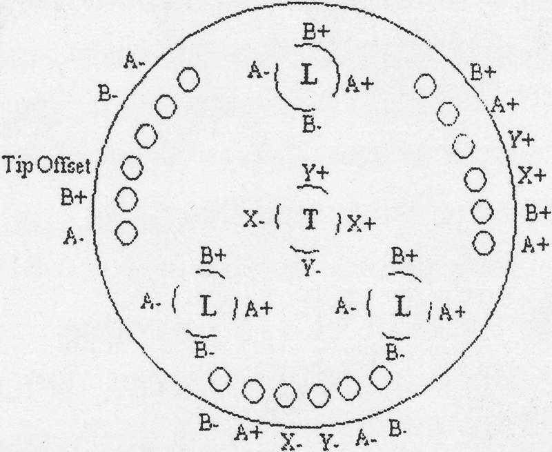
Figure 1. Schematic of electrical connections at the STM head, (bottom view) showing piezo quadrants. L labels the piezo legs and T corresponds to the tip probe. X and Y correspond to connections controlling tip displacement in the plane of the sample surface. A and В correspond to connections controlling rotation of the STM head up and down the ramp.
In order to ensure the samples are properly elevated within the range of tip approach, which is dictated by the ramp for the piezoelectric legs, a set of Ni foils (~ 1 mm each) were used because it is conducting and an available material in our lab. The principal reason for using these foils is because they are sufficiently thin to allow fairly precise control of the sample's height by stacking them together. Each of the Ni foils was attached to one another using graphite tape to avoid displacement between foils. To fix the sample's position, a set of clamps was used, which also promoted better electrical connection between the sample and the ramp's base (see Fig. 3).
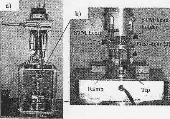
Figure 2. Photograph of the air STM. A) Complete view of the STM-frame and micromanipulator. The total height is 26 in. b) Closer view of the STM piezo-ramp assembly.
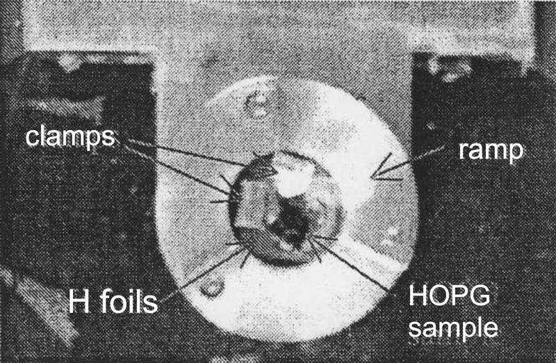
Figure 3. Top-view photograph of the assembly including the ramp, sample, and clamps. The sample shown is HOPG.
Tip Probe
A stable, conducting material that can be formed into a sharp point (ideally 1 atom) is needed for the tip. The most common materials for tip probes are tungsten and Pt/Ir. Commercially available Pt/Ir tips (Nanoprobe™ SPM Tips from Digital Instruments, model PT-ECM) with a total length of 14 mm, were used for this air STM. Pt provides better resistance to oxidation in ambient conditions than tungsten and small amounts of Ir increase the hardness of the tip. The scanning approach mechanism used for this tip was a ceramic piezoelectric material, controlled to have x and у displacements (see Figure 1 and 2b). The tip and the specimen were cleaned only with acetone followed by isopropanol and distilled water. The exposed tip was about 1.5 mm in length. It is ideal to have the exposed tip length as small as possible to avoid vibrational noise.
Electrical Connections and Electronic Design
Electrical connections for the STM head to the piezo tubes and the voltage bias were made with 0.003 in. and 0.010 in. diameter Kapton-coated copper wire, respectively (California Fine Wire, Co.). All wire-wire and wire-pin connections were made using solder and flux (Weller® EC2002M). The electronics used for the computer data input and output was a control module, model V-SCAN 100, and a control panel, model STM 100 from RHK Technology. These electronics are important for surface imaging in one of two ways: 1) in constant height mode, in which the tunneling current is monitored as the tip is scanned parallel to the surface and 2) in constant current mode, in which the tunneling current is maintained constant as the tip is scanned across the surface. In practice, it is most common to image the surface in constant current mode. This is achieved by adjusting the tip's height above the surface so that the tunneling current does not vary with the lateral tip position. For example, in this mode the tip will move slightly upwards as it passes over a surface atom, and conversely, slightly in towards the surface as it passes over a hollow site. This is the major concern of the feedback loop circuit, which is the most critical electronic circuit in the STM design, and is shown in Figure 4.
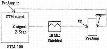
Figure 4. Feedback loop test diagram, which allows monitoring the stability of the STM-100
Vibration Isolation and Noise Control
This section will focus on the main design considerations for the vibration isolation, which includes several methods in order to damp high and low frequency vibrations. Some common sources of noise are: 1) building vibrations due to people walking around at 1 Hz 2) building vibrations due to ventilation, and appliances at 10 to 100 Hz and 3) lowest internal resonance of typical STMs at 1 to 10 kHz.
The basic idea is to make the internal resonance frequencies of the STM very high, and to mount it on a support with a very low resonance frequency. The support will follow only the low-frequency building vibrations and suppress most of the high-frequency components. The remaining low-frequency vibrations, in turn, will not disturb the STM, because they do not introduce any internal motions to the STM (it just moves as a whole structure). In order to damp the frequencies of external vibrations, the present isolation design was accomplished by a stack of stainless steel plates, separated by O-rings, as was used in the first "pocket" STM. Since the elastic material is quite; stiff, the resonance frequencies of the individual stages are quite high. However, the stack of multiple damping stages (each with different resonance frequency, since the supported mass decreases from bottom to top) is quite efficient. The wires for electrical connections as mentioned in the previous section are as thin as possible to reduce noise transmission in the STM. In addition, cardboard was placed around the STM frame to shield it from air currents. To minimize vibration interference, the system was mounted on an air cylinder vibration reducer (Newport, Stabilizer™, 1-2000 Series), which is part of an air-floating floor in order to minimize and damp noise frequencies. The next section of this article shows some results, which reflect the performance of this isolation system.
3. Results
The following section presents the results for an analysis of the vibration reduction provided by the air cylinders and air-floor, and it will show some preliminary images, which indicate successful assembly of the STM and significant reduction of noise. The following vibration analysis of the air STM system was performed using the STM electronic software noise power spectrum acquisition (STM 100 from RHK Technology). Figure 5 a) and b) show the vibration spectra near the air STM with and without the vibration reduction cylinder and floating floor.
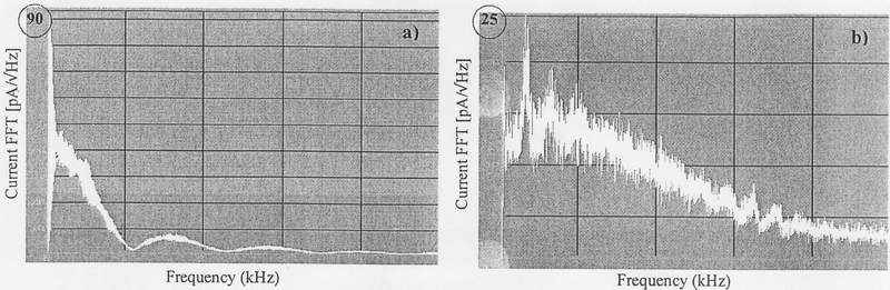
Figure 5. Noise power spectrum for air-SMT : a) without air cylinders and floating floor. b) with air cylinders and floating floor
The above plots demonstrate the expected vibration noise reduction attributed to the air cylinders with the floating floor. Figure 5 a) shows a high intensity at ~ 60 Hz, which is a typical value for appliances and acoustic noises (the maximum intensity at 60Hz is approximately 90 pA/√Hz). Figure 5 b) shows the damped spectrum in the mechanical frequency region (~60Hz) using the air cylinders and the floating floor.
Initial testing of the STM's functionality was performed by scanning a Au(111) surface with a 2° offset. The main purpose of using this Au sample was because it is inert, electrically conducting, and has a high step density. Steps are relatively easy surface defects to image. Some of the results of these scans are shown in Fig. 6. The images indicate the successfully designed and assembled electronics, fine approach mechanism, and piezoelectric leg functionality for the air STM. It is important to mention that the tip used for this measurement was an old tip, which may be damaged due to physical contact on surfaces. A new tip was introduced for future measurements; improved images are expected because it should have a sharper tip. The sample in Figure 6 appears to have some impurities on the surfaces due to previous experimental work.
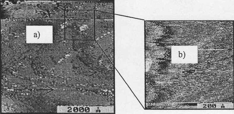
Figure 6. STM image of Au (111) 20 offset surface
The arrows in Fig. 6 a) show the step topography, typical of Au surfaces. Figure 6 b) was a zoom in scan of part of the region shown in Fig. 6 a). In order to accurately determine the resolution obtained with the air-STM, more images need to be acquired.
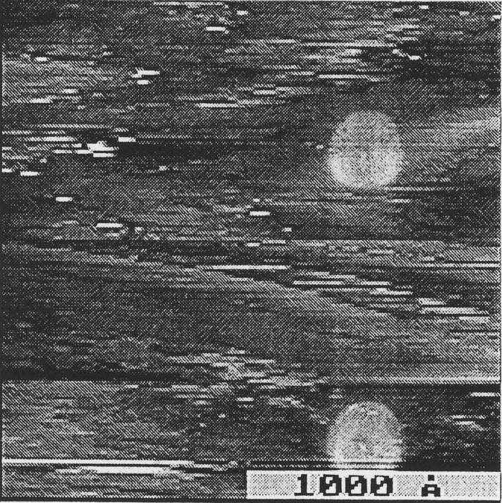
Figure 7. STM image of HOPG surface.
The above figure (Fig. 7) shows the surface structure for the HOPG sample scanned with the air-STM. The surface appears to have a step structure, but more images need to be taken. Future work will include scanning to image the hexagonal structure of HOPG in order to calibrate the scale and optimize the resolution for the air-STM.
4. Conclusions and Outlook
The vibration reduction system shows a reduction in the system vibration, having the expected behavior. The STM was tested by imaging Au(111) 2° offset surface. The air-STM was assembled with success, and minor adjustments to the tip have been made. Present and future work consists of calibrating the air STM using HOPG. Future work will also focus on the tunneling characteristics of charge effects in the air STM. Several investigations have shown the great influence of ambient humidity, giving rise to significant surface conductivity even on insulators. The successful design and assembly of this air STM design will provide a tool to characterize atomically thin films such as graphene.
Аннотация
Рассматривается сканирующий туннельный микроскоп на воздушной подушке для исследования тонких пленок на атомарном уровне в автоматическом режиме в условиях окружающей среды в сравнении с микроскопом с вакуумной системой. Приводится описание конструкции микроскопа для гашения вибраций, электронной части с обратной связью и способа подвода датчика к объекту контроля. Описывается эксперимент контроля пленки Au (111).
Реферат
Рассматривают туннельный микроскоп для сканирования двухмерных материалов на атомарном уровне. Основное преимущество использования микроскопа с воздушной подушкой над микроскопом с вакуумной системой является существенное снижение времени передачи и подготовки образца для сканирования. Микроскоп с воздушной подушкой дешевле, прост в использовании и обслуживании. Элементы конструкции, воздушная подушка и решения при проектировании микроскопа позволяют гасить высокие и низкие частоты вибраций. Вибрационный анализ системы с помощью ПО показывает эффективность использования воздушного цилиндра для снижения вибрации и воздушной подушки. Малый размер датчика устраняет возможность вибрационного шума. В вертикальной и горизонтальной плоскости датчик перемещается микроманипулятором. Конструкция из трех керамических пьезоэлектрических трубок отвечает за точный подвод датчика к объекту контроля. Поверхность сканируют в режиме постоянного тока путем настройки зазора между датчиком и поверхностью контроля. Туннельный ток устраняют боковым перемещением датчика. Обратная связь в схеме микроскопа отвечает за стабильность сканирования. Испытания работы систем микроскопа на золотой пленке Au (111) со смещением 20 подтвердили преимущества конструкции, электронной части и механизма подвода датчика. Микроскоп применяют для контроля тонких пленок на атомарном уровне в автоматическом режиме.